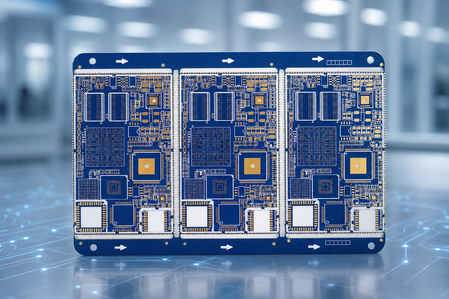
The PCB multilayer manufacturing process is the controlled fabrication flow used to build printed circuit boards with three or more conductive copper layers separated by insulating dielectric materials. It allows compact routing, controlled impedance, better signal integrity and higher assembly density for industrial control, medical electronics, communication devices, automotive electronics and consumer products. For buyers, multilayer PCB manufacturing is not only about layer count. Stackup design, laminate selection, registration accuracy, lamination control, via quality, impedance control and final inspection all determine whether the board can perform reliably. HUIHE Circuits provides Multilayer & Double Sided PCB fabrication services for customers who need reliable multilayer PCB prototypes and production boards.
What Is the PCB Multilayer Manufacturing Process?
The PCB multilayer manufacturing process is a sequence of imaging, etching, lamination, drilling, plating, solder mask, surface finish and electrical testing steps used to form a complete multilayer circuit board.
A multilayer PCB is built by stacking etched inner copper layers with prepreg and core materials, then pressing them together under controlled heat and pressure. After lamination, vias are drilled and plated to connect selected layers. Common multilayer boards include 4-layer, 6-layer, 8-layer, 10-layer and 12-layer structures, while HDI designs may add blind vias, buried vias or sequential lamination. For buyers evaluating a china multilayer pcb supplier, these layer-building capabilities should be confirmed together with registration accuracy, lamination control and supported via structures.
IPC notes that IPC-6012 rigid printed board requirements cover rigid boards including multilayer printed boards with plated-through holes, blind vias, buried vias and microvias. This makes IPC-6012 an important reference when buyers specify quality expectations for multilayer PCB fabrication.
Step-by-Step Multilayer PCB Fabrication Flow
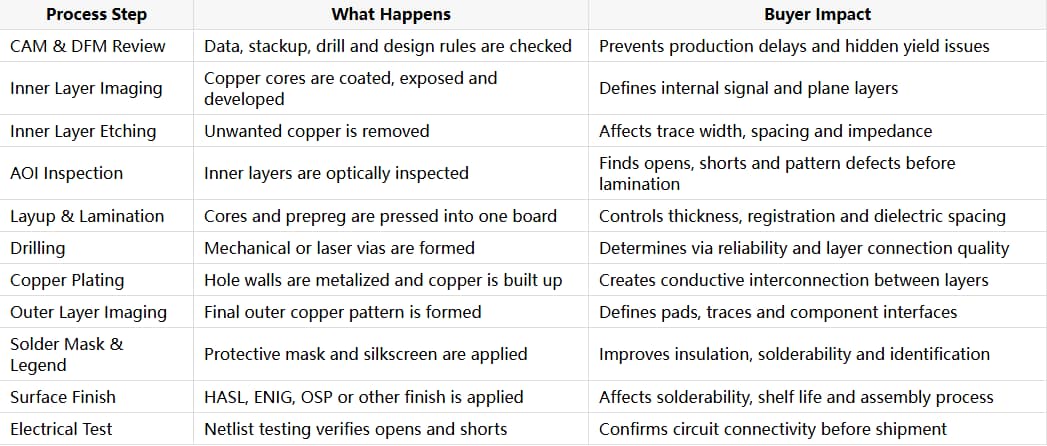
The multilayer PCB fabrication flow is the practical production route that transforms engineering data into a finished bare board ready for assembly. The process usually begins with CAM engineering and DFM review. The manufacturer checks Gerber, ODB++, IPC-2581, drill files, stackup, impedance requirements, copper thickness, solder mask, surface finish and special notes. For high volume pcb fabrication, this pre-production review is especially important because minor stackup, drill or design-rule issues can affect yield across the entire production lot. IPC’s board design standards help designers define manufacturable board requirements before production starts. IPC’s board design standards help designers define manufacturable board requirements before production starts.
HUIHE Circuits’ PCB capability pages show multilayer PCB examples with 4/4 mil, 5/4 mil and 7/4 mil trace/space ranges, board thickness around 0.8–1.6 mm, and minimum hole diameters such as 0.2–0.3 mm depending on the product type.
Quality Control and Process Risks in Multilayer PCB Manufacturing
Quality control in multilayer PCB manufacturing is the system of inspections and process controls used to prevent hidden defects such as delamination, misregistration, via failure, impedance drift and electrical opens or shorts. The most critical risks happen before the board is visible from the outside. Inner-layer defects, poor oxide treatment, resin starvation, voids, drill smear and plating defects can reduce reliability even when the surface looks normal. This is why inner-layer AOI, lamination control, microsection analysis, copper thickness checks, impedance testing and electrical testing are important.
For high-speed designs, controlled impedance should be planned before fabrication, not adjusted after production. These controls are particularly important for a communication pcb, where trace geometry, dielectric thickness and material consistency directly affect signal transmission performance. HUIHE Circuits offers impedance control pcb manufacturing and states that impedance trace tolerance can reach ≤±5% for applications such as high-frequency, high-speed and 5G communication equipment.
For HDI and compact electronics, via structure also affects manufacturability. HUIHE Circuits provides Blind Buried Vias & HDI PCB options, including multilayer examples such as 8-layer, 10-layer and 12-layer boards with blind or buried via processes.
UL explains that PCB recognition and safety compliance testing help verify that PCB materials and constructions meet recognized reliability and safety programs. Buyers developing regulated products should confirm whether material, flammability, traceability or UL marking requirements apply to their PCB project.
Conclusion
The PCB multilayer manufacturing process combines engineering review, inner-layer patterning, lamination, drilling, plating, surface finishing and final testing into one controlled production flow. Each step affects reliability, so buyers should review more than price and lead time when choosing a PCB supplier. For stable multilayer PCB production, the most important buyer inputs are complete fabrication files, clear stackup, material requirements, copper thickness, impedance targets, via structure, surface finish and acceptance standard. HUIHE Circuits supports multilayer PCB, impedance control PCB, HDI PCB and application-focused circuit board manufacturing for industrial control, medical, communication, rail transit and consumer electronics projects.
FAQ
1. What is the multilayer PCB manufacturing process?
It is the process of fabricating a PCB with multiple copper layers by imaging inner layers, etching copper, laminating cores and prepregs, drilling vias, plating holes, finishing surfaces and electrically testing the board.
2. How many layers can a multilayer PCB have?
Common multilayer PCBs include 4, 6, 8, 10 and 12 layers. More complex designs can use higher layer counts, depending on routing density, signal integrity and manufacturer capability.
3. Why is lamination important in multilayer PCB manufacturing?
Lamination bonds copper cores and prepreg into one structure. Poor lamination can cause delamination, thickness variation, registration problems and reliability issues.
4. What files are needed for multilayer PCB fabrication?
Buyers should provide Gerber or ODB++ files, drill files, stackup drawing, impedance requirements, material specification, copper thickness, surface finish, solder mask color and fabrication notes.
5. What is the difference between standard multilayer PCB and HDI PCB?
A standard multilayer PCB usually uses through vias, while HDI PCB may use blind vias, buried vias, microvias and sequential lamination for higher routing density and smaller products.
6. Why choose HUIHE Circuits for multilayer PCB manufacturing?
HUIHE Circuits provides multilayer PCB fabrication, impedance control PCB, HDI PCB and application-specific PCB manufacturing with advanced production equipment, process control and experience serving industrial, medical, communication and consumer electronics customers.
Leave A Comment